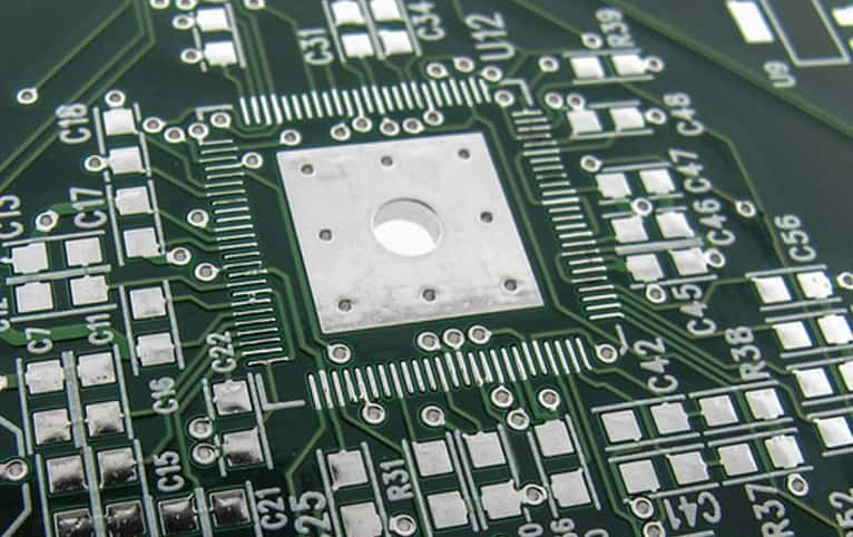
The tin plating (Hot Air Solder Leveling, HASL) process has unique characteristics and significant advantages. HASL is a process in which the assembled PCB is dipped into molten solder (usually a tin/lead alloy) and then leveled off using a hot air knife, which removes excess solder. This leaves a thin and uniform coating of solder on the exposed copper traces and pads, preparing them for subsequent soldering processes in electronic assembly. The result is a robust and reliable finish that has been favored in the industry for many years.

Characteristics of the Tin Plating (HASL) Process
Good solderability
The PCB surface after tin plating has excellent solderability. The tin layer can combine well with the solder to ensure that electronic components can be firmly connected to the PCB during the soldering process. This is crucial for ensuring the quality and reliability of electronic products.
Uniform coating
The HASL process can form a uniform tin coating on the PCB surface. This uniformity helps improve the consistency and stability of soldering and reduces the occurrence of soldering defects.
Relatively low cost
Compared with some other PCB surface treatment methods, the tin plating (HASL) process has a relatively low cost. This makes it widely used in PCB production of various scales.
Adapt to different PCB designs
Whether it is a simple single-sided PCB or a complex multilayer PCB, the HASL process can adapt to different PCB design requirements. It can handle PCBs of various shapes and sizes, providing greater flexibility for designers.
Advantages of the Tin Plating (HASL) Process
Good thermal stability
Tin has a high melting point and good thermal stability. During the operation of electronic products, even in high-temperature environments, the tin plating layer can remain stable and not easily melt or deform. This helps ensure the long-term stable operation of electronic products.
Antioxidant property
The tin plating layer can effectively prevent the oxidation of the copper layer on the PCB surface. Oxidation can lead to a decrease in the solderability of the PCB and affect the soldering quality of electronic components. The PCB surface after tin plating can resist oxidation and maintain good solderability.
Easy to repair
If there are soldering problems during the production or use of electronic products, PCBs treated with tin plating (HASL) are relatively easy to repair. Fault points can be repaired by reheating and soldering without causing serious damage to the PCB.
Mature process technology
The tin plating (HASL) process is a relatively mature PCB surface treatment technology. After years of development and application, its process parameters and quality control methods have been very perfect. This enables manufacturers to stably produce high-quality PCBs.
In conclusion, the tin plating (HASL) process, as an important PCB surface treatment method, has characteristics such as good solderability, uniform coating, low cost, and adaptation to different designs, as well as advantages such as good thermal stability, antioxidant property, easy repair, and mature process technology. In the manufacturing process of PCBs, choosing the appropriate surface treatment method is crucial for improving the quality and reliability of electronic products. The tin plating (HASL) process is undoubtedly a worthy choice.

