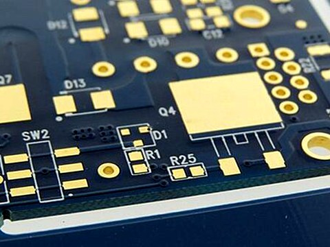
The electroless nickel immersion gold (ENIG) process has become the preferred surface treatment method for many high-end electronic products.Renowned for its dual-layer metallic coating—nickel and a thin layer of gold—ENIG offers a lead-free, environmentally friendly alternative to traditional finishes. The process involves depositing 2 to 8 microns of gold over a 120 to 240 micron nickel layer, which acts as a barrier to copper diffusion and provides a robust soldering surface.

Characteristics of the Electroless Nickel Immersion Gold (ENIG) Process
Good flatness
The ENIG process can form a very flat nickel-gold coating on the PCB surface. This is crucial for the soldering of fine-pitch electronic components, ensuring good contact and reliable connection.
The ENIG process can form a very flat nickel-gold coating on the PCB surface. This is crucial for the soldering of fine-pitch electronic components, ensuring good contact and reliable connection.
Excellent solderability
The nickel-gold coating has excellent solderability and can combine well with various solders. Whether in wave soldering or reflow soldering processes, it can ensure the firm soldering of electronic components and improve the quality and reliability of electronic products.
The nickel-gold coating has excellent solderability and can combine well with various solders. Whether in wave soldering or reflow soldering processes, it can ensure the firm soldering of electronic components and improve the quality and reliability of electronic products.
Good corrosion resistance
The nickel layer, as the bottom layer, has good corrosion resistance and can effectively protect the copper layer on the PCB surface from erosion by the external environment. The gold layer further improves the corrosion resistance and also has good oxidation resistance, ensuring the stable performance of the PCB during long-term use.
The nickel layer, as the bottom layer, has good corrosion resistance and can effectively protect the copper layer on the PCB surface from erosion by the external environment. The gold layer further improves the corrosion resistance and also has good oxidation resistance, ensuring the stable performance of the PCB during long-term use.
Low contact resistance
The contact resistance of the ENIG coating is very low, which is crucial for high-speed signal transmission and high-frequency electronic devices. Low contact resistance can reduce signal loss and improve the performance and stability of electronic devices.
The contact resistance of the ENIG coating is very low, which is crucial for high-speed signal transmission and high-frequency electronic devices. Low contact resistance can reduce signal loss and improve the performance and stability of electronic devices.
Advantages of the Electroless Nickel Immersion Gold (ENIG) Process
Suitable for high-density packaging
With the continuous miniaturization and integration of electronic products, the requirements for PCB surface treatment are getting higher and higher. The ENIG process can meet the needs of high-density packaging and is suitable for advanced packaging technologies such as ball grid arrays (BGAs) and chip-scale packages (CSPs).
With the continuous miniaturization and integration of electronic products, the requirements for PCB surface treatment are getting higher and higher. The ENIG process can meet the needs of high-density packaging and is suitable for advanced packaging technologies such as ball grid arrays (BGAs) and chip-scale packages (CSPs).
Reliable connection performance
Due to the good solderability and corrosion resistance of the nickel-gold coating, PCBs treated with ENIG can provide reliable connection performance. Even in harsh environmental conditions, it can ensure the stable connection of electronic components and improve the reliability and service life of electronic products.
Due to the good solderability and corrosion resistance of the nickel-gold coating, PCBs treated with ENIG can provide reliable connection performance. Even in harsh environmental conditions, it can ensure the stable connection of electronic components and improve the reliability and service life of electronic products.
Aesthetic appearance
The gold layer has good luster and color, making the PCB surface look more beautiful. This is of great significance for some electronic products with high appearance requirements, such as high-end smartphones and tablet computers.
The gold layer has good luster and color, making the PCB surface look more beautiful. This is of great significance for some electronic products with high appearance requirements, such as high-end smartphones and tablet computers.
Environmental friendliness
Compared with some traditional surface treatment processes, the ENIG process is more environmentally friendly. It does not contain harmful substances such as lead and meets the environmental protection requirements of modern electronic products.
Compared with some traditional surface treatment processes, the ENIG process is more environmentally friendly. It does not contain harmful substances such as lead and meets the environmental protection requirements of modern electronic products.
In conclusion, the electroless nickel immersion gold (ENIG) process, with its good flatness, excellent solderability, corrosion resistance, low contact resistance and other characteristics, as well as its advantages such as suitability for high-density packaging, reliable connection performance, aesthetic appearance and environmental friendliness, occupies an important position in the field of PCB surface treatment. With the continuous development and progress of electronic products, the ENIG process will continue to play its important role and contribute to the development of the electronics industry.
