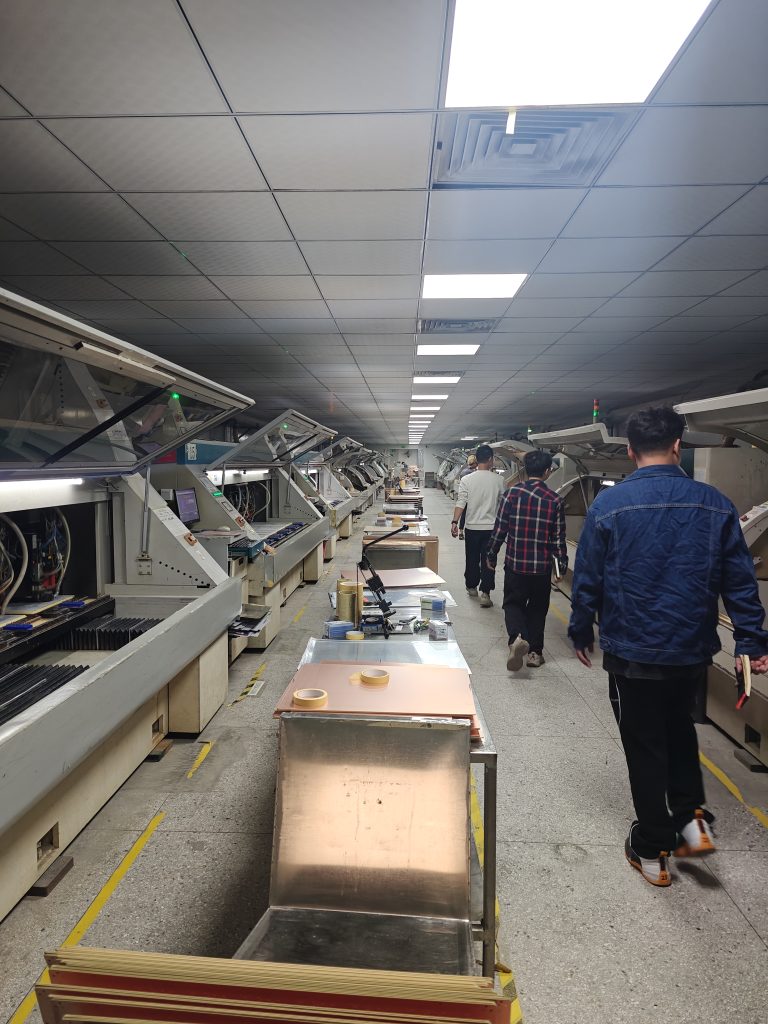
In the world of electronic devices, printed circuit boards (PCBs) play a crucial role. It is like the “home” of electronic components, providing them with stable support and reliable electrical connections.

Insulating Layer
The insulating layer is the foundation of a PCB. Its main function is to isolate different conductive layers and prevent short circuits.
Common insulating materials include epoxy resin and glass fiber. These have good electrical insulation, mechanical strength, and heat resistance.
For example, FR-4 is widely used. It’s composed of glass fiber cloth and epoxy resin. FR-4 has high strength and heat resistance for stable performance.
The thickness of the insulating layer depends on PCB design and application. A thinner one saves space for miniaturized products. A thicker one offers better insulation and strength.
Conductive Layer
The conductive layer is key for electrical connections on a PCB. Usually made of copper foil, it forms circuit patterns through etching.
There are different thickness specs like 18μm and 35μm. Thicker copper foil is for high-power circuits. Thinner is for high-density wiring.
Circuit pattern design considers signal stability and anti-interference. Engineers use EDA software for precise layout and routing.
To improve performance, surface treatments like tin plating and electroless nickel plating with gold enhance solderability and corrosion resistance.
Pads
Pads are metal areas on a PCB for soldering components. Shapes and sizes match component pins and soldering needs.
Common shapes are circular, square, and oval. Made of copper foil, they have surface treatment for good solderability.
During soldering, pads and component pins connect via solder for electrical connection.
Pad layout is crucial for PCB assembly quality and reliability. Reasonable layout eases soldering and reduces defects. It also improves heat dissipation.
Vias
Vias are channels in a PCB for connecting different layers. There are through vias, blind vias, and buried vias.
Through vias penetrate the entire PCB. Blind vias connect outer and inner layers with one end open. Buried vias are in the inner layer for complex connections.
Vias design considers signal quality and impedance matching. Diameter and spacing affect PCB performance and wiring density.
In high-speed circuits, vias’ parasitic capacitance and inductance may affect signal transmission. Optimized design reduces these parasitic parameters.
In conclusion, insulating layer, conductive layer, pads, and vias form the basic structure of a PCB. Each part has a specific role and they cooperate for stable support and reliable connections. In PCB design and manufacturing, consider their characteristics and requirements for performance, quality, and reliability.
