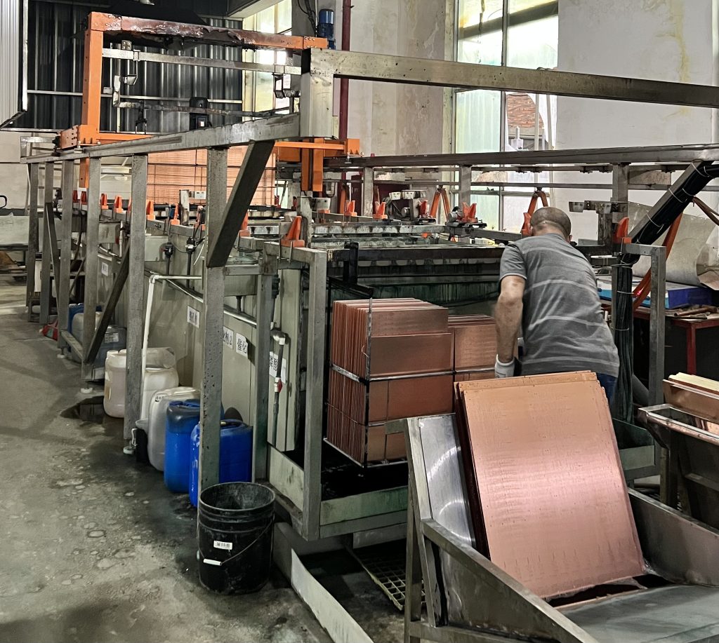
The Plated Through Hole (PTH) process is crucial in PCB manufacturing. It enables connectivity between layers by depositing a thin copper layer on the non-conductive walls of drilled holes. Here’s a closer look at the steps involved:

- Alkaline Cleaning: Removes oils, fingerprints, and dust from the board. This step adjusts the charge on hole walls to aid in copper adhesion.
- Micro-Etching: Cleans and roughens the board surface, enhancing the bond between the base copper and the plated copper layer.
- Pre-Dip and Activation: Protects the activator bath from contamination. It also prepares the hole wall for better adhesion of colloidal palladium, the catalyst for the copper deposit.
- De-Smearing: Removes resin and prepares the hole for uniform copper coverage.
- Copper Deposition: Begins the copper layer buildup, using the catalyst to form an even, conductive coating inside the holes.
The Plated Through Hole (PTH) process is a fundamental step in PCB manufacturing, especially for products requiring high reliability and conductivity. At Amission, our PTH process starts with thorough cleaning and etching to prepare the non-conductive hole walls, followed by activation with a palladium catalyst to ensure strong adhesion. A controlled copper layer is then deposited, creating a conductive path for subsequent electroplating stages, achieving the optimal thickness to meet your specific requirements. With years of experience and certifications like UL, ISO 9001, and ISO 14001, Amission ensures high-quality, precise, and reliable PTH copper plating. Choosing us means partnering with a team dedicated to quality, efficiency, and the meticulous standards your projects demand.
