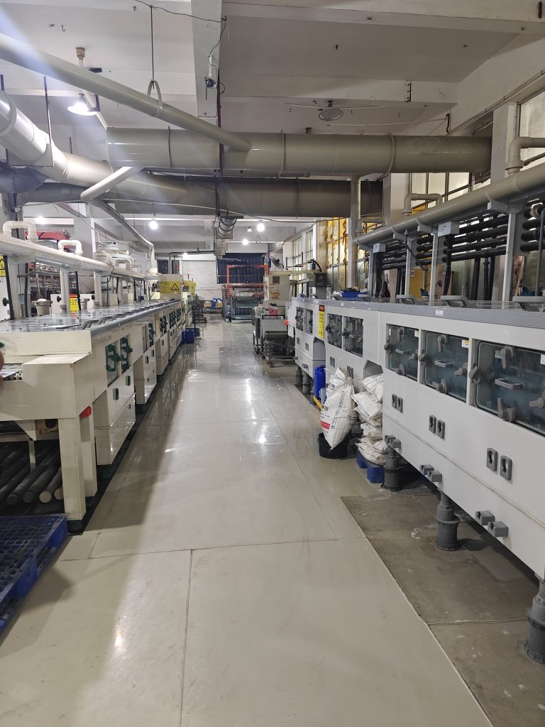
PCB etching process can be designed to transfer the circuit pattern from the copper-clad plate accurately, for the installation of electronic components and connectivity to provide the basis.

The principle of the etching process
Etching is a process of removing material by chemical or physical means. Chemical etching is usually used. The principle is to use a specific etchant and copper cladding board on the unwanted copper foil chemical reaction to dissolve it away, thus leaving the desired circuit pattern.
The etching process can be divided into two main stages: first, the etchant reacts chemically with the surface of the copper foil to form soluble copper compounds; then, these copper compounds are carried away by the etchant, exposing the insulating layer underneath.
The common etching process methods
Acid etching
-
- Acid etching is one of the most commonly used PCB etching methods. It uses acidic etchant, such as ferric chloride, copper chloride, etc., and copper foil chemical reaction. Acid etchant has the advantages of fast etching speed and low cost.
- In the acid etching process, the concentration of etchant, temperature, and etching time need to be controlled to ensure the precision and quality of the etching. At the same time, it is also necessary to carry out appropriate stirring to ensure that the etchant can uniformly contact the surface of the copper foil.
- After acid etching, the PCB board needs to be cleaned and dried to remove residual etchant and other impurities.
Alkaline Etching
-
- Alkaline etching is also a common PCB etching method. It uses an alkaline etchant, such as sodium hydroxide, potassium hydroxide, etc., which reacts chemically with the copper foil. Alkaline etching agent has a slower etching speed, but the etching effect has more uniform characteristics.
- In the alkaline etching process, it is also necessary to control the concentration of etchant, temperature, and etching time. Unlike acid etching, PCB boards after alkaline etching need to be neutralized to remove residual alkaline etchant.
Spray Etching
-
- Spray etching is a method of etching PCB boards by spraying the etchant onto the board in a spray pattern. This method improves the efficiency and uniformity of the etching and is particularly suitable for mass production.
- Spray etching requires the use of specialized spray equipment to spray the etchant evenly onto the surface of the PCB board. In the spraying process, you need to control the spray pressure, flow angle, and other parameters to ensure the effect of etching.
The key factors in the etching process
Etching agent selection
-
- In the choice of etchant, one needs to take into account the PCB design requirements, material properties production efficiency, and other factors. For example, for high-precision PCB manufacturing, you need to choose a slower etching speed, but the etching effect is more uniform etchant.
Control of etching parameters
-
- Etching parameters include etchant concentration, temperature, etching time, spray pressure, and so on. The control of these parameters directly affects the accuracy and quality of etching. In the production process, the best etching parameters need to be determined through experimentation and optimization.
Quality of the resist layer
-
- The resist layer is a layer of material that protects the desired circuit pattern from being etched away during the etching process. The quality of the resist layer directly affects the precision and quality of the etching. In the production of the resist layer, need to ensure that its thickness is uniform, has strong adhesion, good etching resistance.
The quality control of the etching process
Appearance check
-
- After etching the PCB board needs to carry out appearance checks, check whether there is residual copper foil, uneven etching, short circuit, and other issues. Appearance inspection can be carried out through visual observation or the use of microscopes and other tools.
Dimension Measurement
-
- The size of the etched PCB board is measured to check whether the line width, spacing, and other dimensions meet the design requirements. Dimensional measurements can be made with calipers, projectors, and other tools.
Electrical Performance Test
-
- Electrical performance test on the etched PCB board, check its insulation resistance, on-resistance, and other electrical parameters to meet the requirements. Electrical performance tests can use a multimeter, oscilloscope, and other tools.
The PCB etching process is a complex and critical manufacturing process. Through a reasonable choice of etchant, control etching parameters, to ensure the quality of the resist layer, and strict quality control, you can produce high-quality PCB boards, for the performance and reliability of electronic equipment to provide protection.
