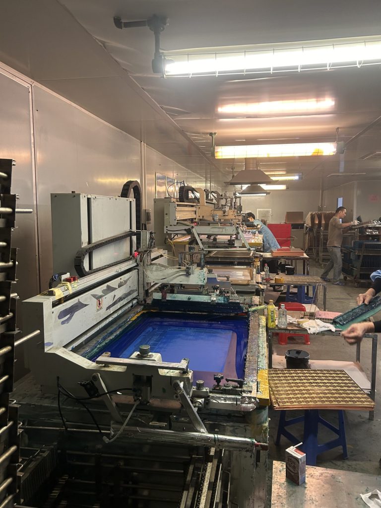
PCB Soldermask not only protects the PCB but also improves its aesthetics and electrical performance.

Definition and Role of Solder Resistance
Soldermask, also known as anti-solder or green paint, is a special coating applied to the PCB surface. Its main functions are as follows:
- Prevent short-circuit: Soldermask can effectively prevent accidental electrical connections between different lines on the PCB, thus avoiding short-circuit failures.
- Protecting the lines: It protects the copper lines on the PCB from oxidation, corrosion and mechanical damage, and extends the service life of the PCB.
- Improves electrical performance: It improves the electrical performance and signal integrity of the PCB by reducing capacitive and inductive coupling between lines.
- Easy to weld: in the welding process, a solder mask can help determine the welding position, and improve the accuracy and efficiency of welding.
Types of Solder Resist Processes
Ink Soldermask
- This is the most common solder mask process. The use of special solder mask ink, through screen printing or spraying the way coated on the PCB surface. Then, after drying and exposure processes, the ink cured to form a solder mask layer.
- Advantages: lower cost, various color options, and different colors that can be customized according to customer needs.
- Disadvantages: Coverage of fine lines may not be uniform and may affect the appearance of the PCB.
Dry Film Soldermask
- A dry film solder mask is a dry film that is first attached to the PCB surface and then exposed and developed to form a solder mask layer.
- Advantages: Can provide more uniform coverage, and better protection for fine lines.
- Disadvantages: high cost, relatively complex operation, and the need for specialized equipment and technology.
Solder Resist Steps
Surface treatment
- Before coating the solder mask, the PCB surface needs to be cleaned and treated to ensure that the solder mask can adhere well. Usually use methods such as pickling, and micro-etching.
Ink or Dry Film Coating
- Depending on the type of solder mask process selected, the solder mask is applied to the PCB surface by screen printing, spraying, or dry film application.
Drying
- The coated PCB needs to be dried to remove solvents from the solder mask and to allow for initial curing.
Exposure
- Exposure is required for PCBs that use ink solder masks. The PCB is placed under an exposure machine and a specific pattern is irradiated onto the solder mask through a photomask, causing a chemical reaction in the irradiated portion, which is retained in the subsequent development process.
Developing
- The exposed PCB is placed into the developer solution and the unexposed portion is dissolved away, revealing the areas and wiring to be soldered.
Curing
- After the development of the PCB for the final curing process, the solder mask is completely cured to achieve the required hardness and wear resistance.
Quality control of the solder mask process
Appearance Inspection
- Check whether the color of the solder mask is uniform and, if there are no bubbles, pinholes, scratches, and other defects.
Thickness measurement
- Use professional instruments to measure the thickness of the solder resist layer to ensure that it meets the design requirements. Too thin a solder mask may not provide sufficient protection, while too thick a layer may affect the electrical performance of the PCB.
Adhesion Test
- Adhesion of the solder mask to the PCB surface is tested by taping and peeling tests to ensure that the solder mask will not come off during use.
Electrical Performance Test
- Use professional test equipment to test the electrical performance of the PCB to check whether the solder mask has any adverse effect on the electrical performance.
PCB solder mask is an indispensable part of the PCB manufacturing process. Choosing the right type of solder mask process and strictly controlling the process steps and quality, can provide good protection for the PCB, improve its aesthetics and electrical performance, and ensure the stable operation of electronic products.
