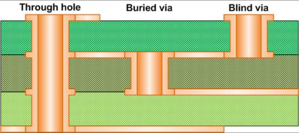
PCB vias play a vital role in connectivity. Among them, through holes, blind holes, and buried holes are three common types of guide holes,which have their own characteristics and application scenarios.

Through Hole
Definition and structure
- Through Hole is a guide hole that runs through the entire PCB board, from the top layer all the way to the bottom layer. It is usually processed by mechanical drilling or laser drilling.
- The inside of the through hole is usually plated with a layer of metal, such as copper, to ensure good electrical conductivity.
Features & Benefits
- Strong connectivity: Through-holes enable full connectivity between multiple PCB layers. Whether power, signal, or ground, it can be reliably transmitted through the through-hole.
- Mature technology: Through-hole processing technology is relatively mature and low-cost. It can be easily realized by most PCB manufacturers.
- Easy to inspect and repair: Since the through-hole runs through the entire PCB, it is relatively easy to inspect and repair. Simple measuring tools and methods can be used to determine whether the through-hole connection is good or not.
Application Scenarios
-
- For some cost-sensitive, relatively simple design electronic products, a through-hole is a common type of guide hole. For example, some household appliances, and industrial control equipment.
Blind Via
Definition and structure
-
- Blind holes are vias that connect the outer and inner layers of a PCB, with one end open and the other closed inside the PCB. Blind holes are usually processed by laser drilling or mechanical drilling and then plating.
- The depth of the blind vias is usually less than the thickness of the PCB but can be different depending on the design requirements.
Features & Benefits
-
- Space-saving: Blind vias connect only specific inner and outer layers. This saves space by reducing the number of layers and thickness of the PCB compared to through-holes. It is suitable for some miniaturized and high-density electronic products.
- Reduced signal interference: Due to the shorter length of the blind vias, the signal loss and interference during transmission are relatively small, which helps to improve the performance of the circuit.
- Good aesthetics: Blind vias do not have obvious holes on both sides of the PCB like through holes, which makes the appearance of the PCB cleaner and more aesthetically pleasing.
Application Scenarios
-
- Blind vias are widely used in miniaturized and high-performance electronic products such as high-end smartphones, tablet PCs, and laptops.
Buried Via
Definition and structure
-
- Buried holes are guide holes that are completely buried between the inner layers of the PCB and are not connected to the outer layers of the PCB. Buried holes are usually formed in the lamination process of multi-layer PCBs, and then processed through plating and other processes.
- Submerged vias are difficult to process and require high-precision equipment and process control.
Features and Benefits
-
- Improve wiring density: Buried holes can realize the connection between inner layers without affecting the layout of the outer layers of the PCB, thus improving the wiring density of the PCB, which is suitable for complex high-speed circuit design.
- Enhanced Signal Integrity: Buried holes can reduce reflection and interference during signal transmission, improving signal integrity and stability.
- Good confidentiality: Since the buried holes are not connected to the outer layer, they can provide better confidentiality for some circuit designs that require confidentiality.
Application Scenarios
-
- In aerospace, military electronics, high-end communication equipment, and other areas that require high performance and confidentiality, buried holes are often used.
Summary of the differences between the three types of vias
Connection method
-
- Through holes run through the entire PCB, connecting all layers; blind holes connect the outer and inner layers; buried holes connect only the inner layer.
Visibility
-
- Through holes are visible on both sides of the PCB; blind holes are visible on one side only; buried holes are not visible at all.
Processing Difficulty
-
- Through holes are relatively easy to process; blind holes are moderately difficult; buried holes are the most difficult to process.
Application Scenarios
-
- Through holes are suitable for cost-sensitive, simple-design products; blind holes are suitable for miniaturized, high-density electronic products; buried holes are suitable for areas requiring high performance and confidentiality.
Through holes, blind holes, and buried holes each have their own unique roles and advantages in PCB design and manufacturing. According to different product needs and design requirements, selecting the appropriate type of vias can effectively improve the performance and reliability of the PCB.
