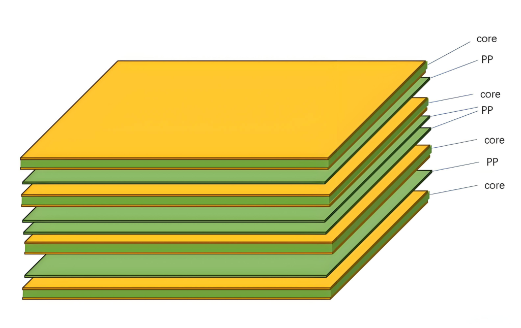
The design of the PCB layer stacking structure has a decisive impact on circuit performance. Proper layer stacking can optimize signal integrity, reduce electromagnetic interference, and improve circuit reliability.

The role of the laminated structure
- Controls transmission line impedance to reduce signal crosstalk and loss.
- Reduces electromagnetic emissions and improves EMC performance.
- Thermal management, is essential for high-heat components and circuits.
Selection of layers
- The number of signals, device density, PIN density, and signal frequency are the key factors in determining the number of layers.
- High-frequency signals or high-density devices usually require multilayer board designs.
Impact of Different Layer Stacks
- 4-layer board: Common structures include S-G-S-G, suitable for low-frequency signals.
- 6-layer board: SIG-GND-SIG-PWR-GND-SIG is recommended to provide better signal integrity.
- 8-layer board: The best structure is S-G-S-P-G-S-G-S-G-S, which provides excellent geomagnetic absorption.
Impedance Control
- Impedance mismatch can lead to signal distortion and radiation.
- Copper thickness, dielectric constant, line width, and line spacing of the alignment all affect the impedance.
Electromagnetic Absorption
- – The use of multi-layer ground reference planes can improve electromagnetic absorption.
- – The spacing between the power and ground layers should be minimized for good power and ground coupling.
Balance of Cost and Performance
- More layers means higher cost.
- A reasonable layer stack design can find a balance between cost and performance.
Conclusion:
PCB layer stack structure design is an important part of circuit performance optimization. With a well-designed layer structure, the performance and reliability of a circuit can be significantly improved while controlling costs.
