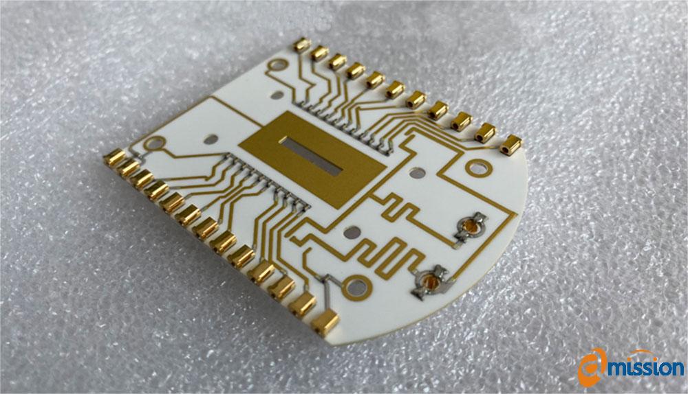
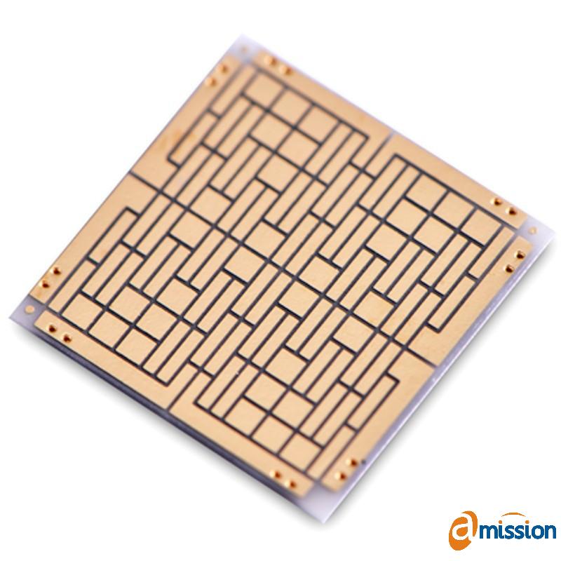
Apart from MCPCB, if your
application requires high pressure, high insulation,
high frequency, high temperature, and high reliability in small electronic
products, Ceramic PCBs are an excellent choice.Why do Ceramic PCBs perform so well? Let's look at their basic structure to
understand.
- Base Material: 96% or 98% Alumina (Al2O3), Aluminum Nitride (ALN), or
Beryllium
Oxide (BeO)
- Conductive Material: For thin and thick film technology, the conductors are
typically silver palladium (AgPd) or gold palladium (AuPd). For Direct
Copper
Bonded (DCB) technology, copper is used.
- Application Temperature Range: -55°C to 850°C
- Thermal Conductivity: 24W-28W/m-K for Al2O3, 150W-240W/m-K for ALN, and
220W-250W/m-K for BeO
- Maximum Compression Strength: Greater than 7,000 N/cm²
- Breakdown Voltage: 15/20/28 KV/mm for thicknesses of 0.25mm, 0.63mm, and
1.0mm
respectively
- Thermal Expansion Coefficient: 7.4 ppm/K (within the range of 50°C to 200°C)
|
| Application of Ceramic PCB |
- High-accuracy clock oscillators, voltage-controlled oscillators (VCXO),
temperature-compensated crystal oscillators (TCXOs), and oven-controlled
crystal oscillators (OCXOs)
- Semiconductor cooler
- Electric power electronic control modules
- High insulation and high-pressure devices
- High-temperature applications (up to 800°C)
- High power LEDs
- High Power semiconductor modules
- Solid-state relay (SSR)
- DC-DC module power sources
- Electric power transmitter modules
- Solar-panel arrays
|
| Ceramic PCB Technics Capacity |
|
No. |
Item |
Description |
DataSheet |
|
1 |
Max Layer Count |
|
Thick Film: 10L; DCB: 2L |
|
2 |
Min Board Thickness |
mm |
Thick Film: 0.25mm
DCB: 0.30mm |
|
mm |
Thick Film: 0.28mm
DCB: 0.40mm |
|
mm |
0.34mm |
|
mm |
0.46mm |
|
mm |
0.81mm |
|
mm |
1.50mm |
|
3 |
Max Board Thickness |
mm |
Thick Film: 1.5mm
DCB: 1L: 1.3mm;
2L 1.6mm |
|
4 |
Max Board Dimension |
mm |
"Thick Film: 200*200mm
DCB: 138*178mm |
|
5 |
Max Conductor Thickness |
|
Thick Film: 13um
DCB: 8.6OZ |
|
6 |
Min Conductor Thickness |
|
Thick Film: 10um
DCB:3.9 OZ |
|
7 |
Min Trace Width/Space |
mil |
Thick Film: 6/8mil
DCB: 12/12mil |
|
8 |
Min Hole Diameter |
mm |
0.1mm |
|
9 |
Min Punch Hole Dia |
|
N/M |
|
10 |
Min Hole Spacing |
mm |
NPTH: 0.30mm
PTH: 0.5mm |
|
11 |
Max Aspect Ratio |
rate |
8:1 |
|
12 |
Min Solder PAD Dia |
mm |
0.25mm |
|
13 |
Min PAD Ring(Single) |
mil |
3mil
6mil
8mil |
|
14 |
PTH Wall Thickness |
|
Thick Film: 10um
DCB: Not Available |
|
15 |
PTH Dia Tolerance |
mil |
± 4 mil |
|
16 |
NPTH Dia Tolerance |
mil |
± 2 mil |
|
17 |
Hole Position |
mil |
±4 mil |
|
18 |
Outline Tolerance |
mm |
Laser: +0.2/0.05mm |
|
mm |
Die Punch: +0.25/0.20mm |
|
19 |
Min Soldermask Bridge |
mil |
2 mil |
|
20 |
Min BAG PAD Margin |
mil |
12 mil |
|
21 |
Impedance Controlled |
|
N/M |
|
22 |
Thermal Conductivity
(W/m.K, or W/m.C) |
|
Al2O3: >= 24 W/C-K
AIN: >=170 W/C-K |
|
23 |
Dielectric Strength |
|
>15 KV/mm |
|
24 |
Wrap & Twist |
|
≤ 3% |
|
25 |
Flammability |
|
94V-0 |
|
26 |
Thermal Stress |
|
3 x 10 Sec @ 280 ℃ |
|
27 |
Surface Treatment |
|
Thick Film: AgPd, AuPd, Mn/Ni
DCB: Ni plating, ENIG |
|
|
Please contact us today for more
information about Ceramic circuit board (Ceramic PCB). |


