| Definition | |
|
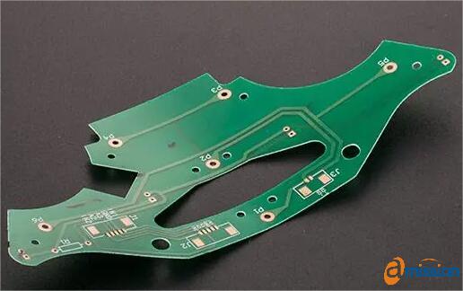
Extra thin printed circuits are boards thinner than the standard PCBs. The typical thickness of a standard PCB ranges from 1.0 mm to 2.0 mm, with a minimum thickness of 0.3 mm or 0.4 mm for 1-layer or 2-layer PCBs. For 4-layer PCBs, the thickness is usually around 0.6 mm. These boards are commonly referred to as thin PCBs or thin boards. |
|
| Thinner Thickness Requirements | |
|
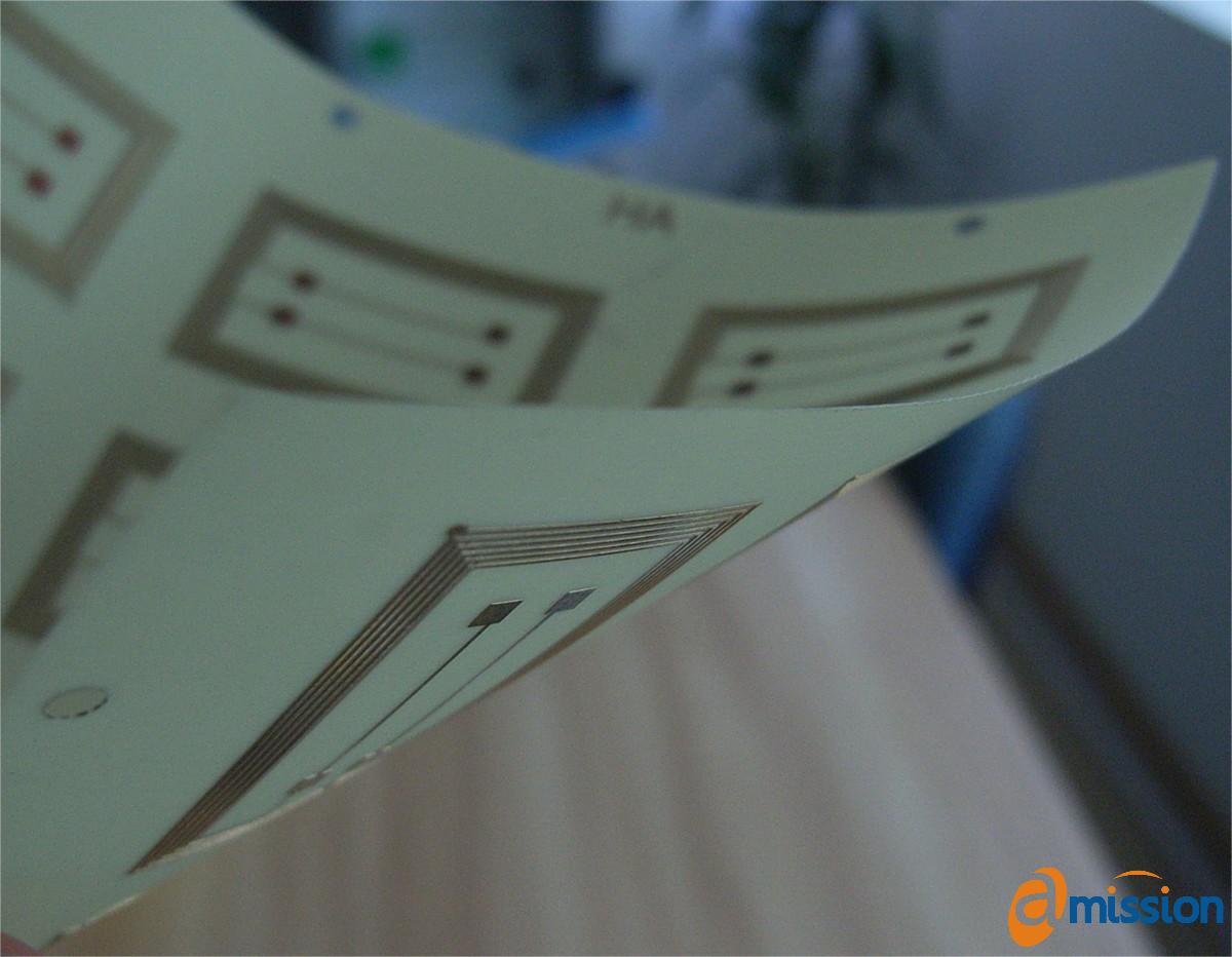
Sometimes, due to space constraints, design requirements, or specific needs, a much thinner thickness is required, such as 0.25 mm, 0.20 mm, or even 0.15 mm. This allows the PCB to be used in applications like SIM cards, sensor cards, and more. Due to their extreme thinness, these are known as extra thin PCBs or very thin PCBs. |
|
| Market Demand and Applications | |
|
With the demand for thinner devices, there is a trend towards making designs more portable, lightweight, and flexible. Consequently, the application of extra thin PCBs is becoming increasingly widespread. |
|
| Features of Extra Thin FR4 PCB | |
|
Extra thin FR4 PCBs can be manufactured as thin as flexible PCBs, offering bendability similar to a flexible circuit, but with more rigidity and at a lower cost compared to boards with the same copper traces. |
|
| Specifications | |
|
For extra thin PCBs, we can produce them in the following thicknesses: 0.15 mm, 0.20 mm, 0.25 mm, 0.30 mm, with or without solder mask, and copper thickness options of ½ OZ, 1 OZ, 2 OZ, 3 OZ. |
|
| Extra Thin Board Capability | |


|
|
| Please contact us for more information about extra thin PCB. | |